- VISION
- - INSIGHT
- - ACTION
ELECTRONS INTO ORDER
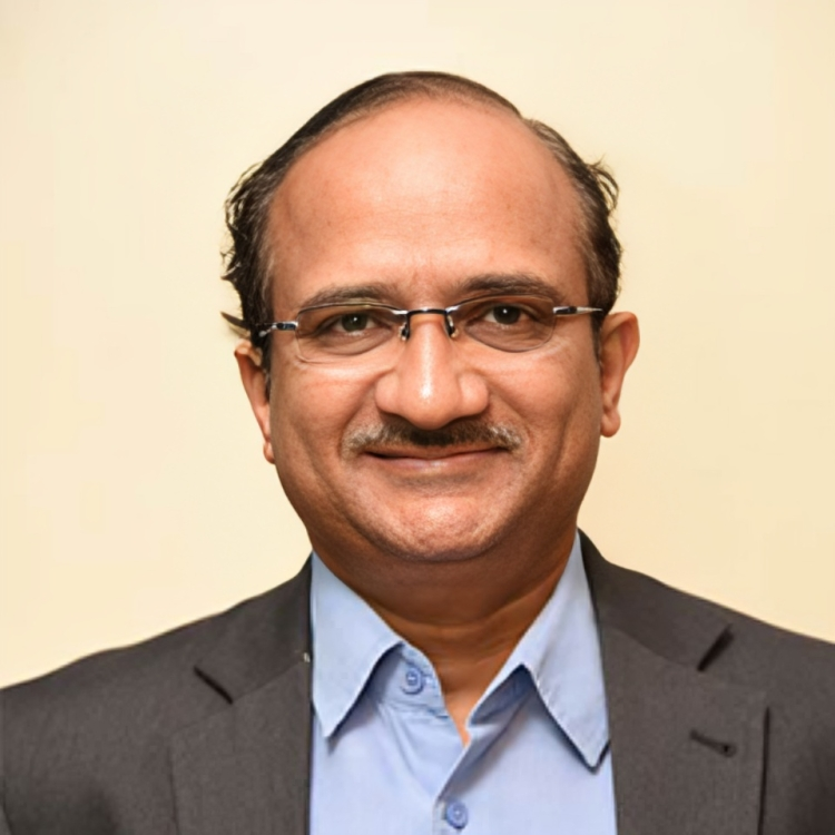
“Prof. V. Ramgopal Rao is a globally recognized nanoelectronics researcher with over 500 publications and 50 patents, including 20 US patents and technologies used in hundreds of millions of chips. He previously served as Director of IIT Delhi from 2016 to 2021 and as a Chair Professor at both IIT Bombay and IIT Delhi. He co-founded two deep tech startups, Nanosniff and Soilsens, and played a key role in establishing India’s major nanoelectronics programs. A Fellow of all major science and engineering academies in India and abroad, he has supervised 52 Ph.D. students and received over 40 national and international honors including the Shanti Swarup Bhatnagar Prize, Infosys Prize and IEEE EDS Education Award. He currently chairs national bodies such as JNCASR and NIFTEM and serves on editorial boards of leading international journals. He is currently the Group Vice Chancellor of BITS Pilani, overseeing its campuses in Pilani, Hyderabad, Goa, Dubai and Mumbai. ”

PROF. V RAMGOPAL RAO
IIT BOMBAY
“No dream is too big if you are willing to start small, stay grounded, and work relentlessly.”
Witness to the Moore’s Law Era: I had the privilege of contributing during the peak years of Moore’s Law, when device scaling and increased component density drove innovation in nanoelectronics. It was a time of tremendous clarity and excitement, where every advancement had a clear goalpost. That era helped shape not only my technical perspective but also my appreciation for structured innovation.
I still remember one of my school teachers who used to bring all the ingredients to class to show us how to make soap. That’s how chemistry first caught my attention. It was small moments like those, growing up in Kollapur between 1972 and 1982, that shaped my curiosity. Coming from a lower-middle-class family, the idea was simple – study well, get a job, and help the family. We had enough, but never excess. Education was the only asset.
We were told that if you want a stable job, become an engineer. That’s how it was in those days. Science and mathematics were my strengths, and there were engineers in the extended family. One of my uncles was a professor at IIT Madras. I looked up to him. Still, after Class 12, I didn’t attempt the IIT entrance exam. My entire schooling was in Telugu, and the exam was in English. It felt like a wall I couldn’t cross.
So I joined Kakatiya University in Warangal for my B.Tech. I liked electronics and instrumentation, and things were going well. But then came a choice that would change everything. After B.Tech., I decided to pursue an M.Tech. at IIT Bombay. That decision altered the course of my life.
At IIT Bombay, the environment was entirely new. The classes were competitive, the peers outstanding, and the learning unmatched. I met Prof. Juzer Vasi there, who introduced me to microelectronics. I often say this – had he been working in communication systems, I may have gone down a different path. But because he worked on devices, I did too. That’s where my interest in electron devices began.
During my M.Tech., I wrote a paper that got published in the Journal of Applied Physics, an American journal of repute. That was rare for an M.Tech. student at the time. The work continued with radiation-hardened devices for ISRO’s satellites. I was involved in developing chips at SCL Chandigarh, a national project led by IIT Bombay. That exposure shaped my thinking. Research was not just about theory – it could also solve real-world problems.
FROM INDIA TO GERMANY AND BACK
After M.Tech., I went to Germany on a DAAD fellowship and joined the University of the Bundeswehr Munich for a Ph.D. I completed it in less than two and half years. Then I moved to UCLA for postdoctoral research. While my M.Tech. focused on radiation hard devices, the Ph.D. shifted to vertical nanometer transistors, and at UCLA, I explored lateral Nano-scale transistors. This seamless transition from one direction to another gave me both depth and continuity.
When I returned to India, I brought those collaborations with me. Many of my early papers had UCLA affiliations because we were using device samples from UCLA, fabricated at Stanford. That gave us access to cutting-edge technologies. In 1998, I joined IIT Bombay as an Assistant Professor. By 2005, I had become a full Professor.
We were among the first in India to publish on sub-100 nanometer devices. Back then, the available technologies were much older. So the papers stood out. I remember one committee member from IISc telling IIT Bombay Director during my promotional interview, “You must recommend him for national awards, he is doing extraordinarily well.” And then came the Swarnajayanti Fellowship in 2004, Shanti Swarup Bhatnagar Prize in 2005, and later, many more.
FINDING PURPOSE BEYOND PUBLICATIONS
Recognitions helped. But over time, I began to feel a sense of discomfort. Most of our work was being used by companies abroad Intel, IBM, Infineon etc. There was no semiconductor manufacturing in India. Our students would go to the US, and our technologies were being commercialized overseas.
This made me reflect. I had come back to India to make a difference here. If everything we did helped only other countries, what was the point? That’s when I started shifting focus, from publishing papers to solving problems that mattered in India.
We began working on sensor technologies – first for early cardiac detection, and then for agriculture and homeland security. That journey led to the founding of Nanosniff and SoilSense, two deep-tech startups. Today, Nanosniff’s trace explosives detection system is deployed at multiple Indian airports. These were research-led products, solving real challenges at home.
In parallel, our CMOS research continued. We licensed several patents to industry. Many of these technologies were used in millions of integrated circuits worldwide. So, while the sensor work made a local impact, the CMOS research helped us leave a global footprint.
What worked for me was not extraordinary brilliance – but persistence and consistency. I often tell students: outwork everyone. It is hard work over long periods that pays off. I chose problems that mattered and stayed with them until something came out of it – papers, patents, or products.
However, today there’s also the issue of incentives. When faculty are judged primarily on the number of publications and citation metrics, the temptation to cut corners increases. The race to publish must be replaced with a race to solve meaningful problems. Institutions must value quality over quantity, depth over speed.
Science in India is at a turning point. To scale our innovations globally, we must first get the foundation right. And that foundation is integrity. Without it, even the best ideas will collapse under the weight of doubt. It’s time to clean up, not cover up.
During my time at IIT Delhi, we made a conscious shift. We launched internal grant mechanisms that prioritized interdisciplinary and impact-led proposals. We gave weightage to societal contributions, not just citation metrics. At BITS Pilani, we are following a similar path – measuring faculty contributions through research impact, not just numbers.
At its core, education is about impact. If an institution helps a village improve crop yields, or builds a tool that saves lives, it must be celebrated. Not just institutions that publish 500 papers. The metrics must evolve. We don’t need more rankings – we need more relevance.
THE MOORE'S LAW ERA AND WHAT CAME NEXT
When I started, Moore’s Law was the beacon. Every 18 months, industry would shrink devices, double the density, and reduce power. It was exhilarating. That era gave structure to innovation. But Moore’s Law has reached its limits. We’re no longer able to shrink transistors in the same way.
Now, the shift is toward heterogeneous integration. Instead of shrinking, we integrate – bringing together processors, memory, analog components, sensors – onto a single chip. That is the future.
But even integration has limits. We need new ideas. One of those ideas is molecular electronics, using molecules to behave like transistors. Making one molecule switch is hard. Making hundreds of them talk to each other to build logic circuits is even harder. But if we can do that, we will redefine computing itself.
Another frontier is energy. AI chips are powerful but consume enormous amounts of power. In the Moore’s Law era, performance increased, but power consumption per operation went down. Now, it’s the opposite. If we keep going like this, we’ll need nuclear reactors just to power servers.
We must innovate not just for speed but for energy efficiency. That will be the biggest constraint in the coming years.
SEMICONDUCTORS AND THE INDIA STORY
India is trying, for the third time, to enter semiconductor manufacturing. The first two attempts didn’t go far. This time, things seem more serious. Micron is setting up a packaging plant. Tata is entering fabrication. These are early steps, but they matter.
We must understand that fabs are only one piece. The entire ecosystem matters chemical suppliers, cleanroom gases, ports, water, power, trained manpower, logistics. Without these, fabs can’t survive.
And then there’s geopolitics. The US controls the tools. Taiwan dominates manufacturing. China is a major player. India has to find a space where it can contribute meaningfully – perhaps in mature nodes, packaging, or advanced design. Design is already our strength. Manufacturing can follow.
What holds us back is not the lack of talent, but the system. Bureaucracy, fragmented policies, and the absence of execution hold us back. We need alignment – between technology, policy, and execution.
DEEP TECH NEEDS DEEP SUPPORT
India’s startup story is impressive, but it’s mostly in services, fintech, and e-commerce. Deep tech is still a missing piece. Less than 5% of Indian unicorns are based on intellectual property. Deep tech needs long-term capital, patient investors, and academic ecosystems that encourage risk.
VCs prefer faster returns. Deep tech doesn’t give that. So, startups struggle after the initial grant phase. Government support is good for prototypes, but private capital is essential to scale.
We must also train students to think beyond placements – to consider entrepreneurship, to take the road less traveled. Faculty must play a role too. Research cannot stop at papers. We need to see ideas through to the market.
CLOSING REFLECTIONS
Today, my time is divided between mentoring students, building institutions, guiding national missions, and occasionally going back to the lab. The thrill of discovery remains, but the purpose has widened. We need more people who can connect research with real-world needs. We need leadership that executes. We need systems that support the long game.
India has the talent. What we need is trust in ourselves, alignment in systems, and courage to back deep ideas. The future belongs to those who can bring science, purpose, and perseverance together.
Date 29.06.2025
Deep Tech, Electron Devices, Nanoelectronics, Semiconductor Innovation, Sensor Technology
